Few people still have their photos developed these days. Yet the use of light to transfer a mask design onto a light-sensitive layer is now at the heart of a very promising field of research… but at the microscale! This is the principle behind photolithography, a fundamental technique used to produce the tiny electronic circuits and components in our connected objects.
Kevin Heggarty has been exploring this technology at IMT Atlantique for nearly twenty years, specifically in the area of parallel photoplotting. The researcher and his team are drawing on their expertise to contribute to the European FABulous project aimed at producing high-resolution 3D microscale optical components with functional surfaces.
Laser writing: from 2D to 3D
Photoplotting or photolithography is the process of using a light beam (laser) or electrons to write patterns onto photosensitive materials, typically photopolymerizable resin. This specific type of resin polymerizes when exposed to light: it goes from a liquid-paste-like state to a solid state. The surface is then rinsed to remove the resin that is still in a liquid state so that only the polymerized resin remains.
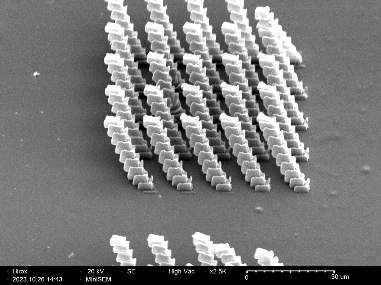
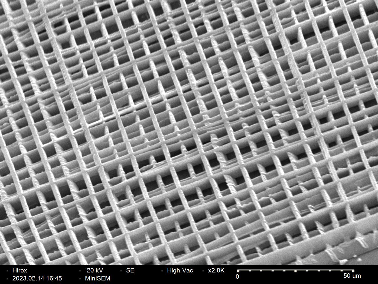
This technique makes it possible to manufacture 2D structures on thin resin layers as well as 3D structures on thicker resin layers, “like a 3D printer,” Kevin Heggarty explains, “but with submicron resolution.” It then requires the use of an ultrafast laser called a femtosecond laser. “These lasers instantaneously increase the light intensity, with the effect of ‘confining’ 3D polymerization. This is not attainable when simple light sources, like LED and conventional lasers are used, since they polymerize everything they come in contact with. It then becomes very difficult, if not impossible, to make high-resolution 3D structures,” the researcher adds. This specific photolithography technique is called multiphoton.
Speeding up photoplotting multiple beams
Although photoplotting technology has been used to write in 2D for nearly forty years, 3D photoplotting has only been marketed for about ten years. The technique has applications in numerous fields, particularly in optics and photonics to manufacture structures the size of a wavelength. It is used, for example, to manufacture color filters and anti-glare filters for automotive cameras. It is also of interest to biologists for the design of micro-nanoscopic scaffolds to help with cell culture. However, the technology is marketed in its single-beam form, meaning that it uses only one beam that plots point by point. “The writing takes a while,” Kevin Heggarty says.
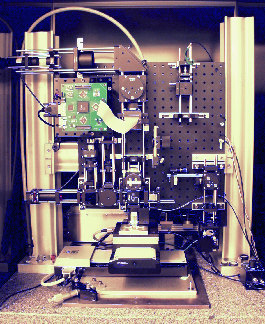
To overcome this obstacle, the researcher and his team dedicated around twenty years of study to a technique that speeds up the process by writing with several laser beams in parallel: parallel photoplotting. Although the process had already been applied to mono-photon (two-dimensional) photoplotting, it had never been combined with multi-photons, that is until recent progress in the field made this possible. After receiving a request for their expertise, Kevin Heggarty’s team joined the PHENOmenon H2020 project “to try to apply our knowledge and skills in the parallelization of the writing process to this new multi-photon lithography technique,” the researcher explains.


